
By Austin ChipFrontier Editorial Team Connecting Innovators and Building Futures Once known primarily for software startups and live music, Austin is rapidly becoming one of the most important semiconductor and high-tech manufacturing centers in the United States. Over the past five years, coordinated actions by the federal government, the State of Texas, and major corporations such as Samsung have turned Central Texas into a hub of innovation, infrastructure, and opportunity. Policy Power: State & Federal Initiatives Fuel the Chip Boom The semiconductor surge began with the CHIPS and Science Act of 2022, a landmark federal law directing billions of dollars toward domestic chipmaking. Through the U.S. Department of Commerce’s CHIPS Incentives Program, leading foundries have secured multibillion-dollar grants to expand U.S. fabrication capacity. One of the largest awards went to Samsung Electronics, which received up to $4.745 billion to build and scale its new Texas cluster – a commitment that places Austin-Taylor among the top advanced-manufacturing centers in the country (U.S. Dept. of Commerce, 2024). At the state level, Texas launched the Texas Semiconductor Innovation Fund (TSIF) – a $698 million initiative to strengthen research, workforce training, and supply-chain infrastructure across the state. The program, established in 2023, funds everything from semiconductor curriculum development to direct company grants, positioning Texas as a national leader in CHIPS-era industrial policy (Texas Governor’s Office, 2023). Local institutions are already benefiting. Austin Community College recently received a TSIF workforce grant to establish a semiconductor manufacturing lab and advanced technician training center – a concrete example of how state policy links education with industry growth. Corporate Catalysts: Samsung and the Rise of a Manufacturing Megacluster The semiconductor transformation of Central Texas is anchored by Samsung’s historic investment in its Taylor and Austin campuses. Announced in 2021, Samsung’s initial Taylor project carried a price tag of $17 billion – one of the largest foreign direct investments in U.S. history. Since then, with CHIPS Act support and expanded plans, total commitments have grown dramatically. Public reports now estimate $37 – $40 billion in cumulative investment across Samsung’s Central Texas cluster (Reuters 2024; Samsung Economic Impact Report 2023). The impact is massive: Samsung’s 2022 economic impact report estimated $13.6 billion in local economic activity tied to its Austin and Taylor facilities – a number that continues to climb as new fabs, suppliers, and training centers come online. Meanwhile, other semiconductor and adjacent tech companies – from Texas Instruments to Applied Materials and a growing base of specialty chemical, equipment, and AI-hardware suppliers – are expanding their footprint in Texas. This multiplier effect is creating a dense, interlinked ecosystem that strengthens the region’s global competitiveness. The Austin Effect: Jobs, Growth & Societal Impact According to the U.S. Department of Labor, semiconductor manufacturing investments in Central Texas are projected to create over 25,000 high-paying jobs by 2030 – including construction, operations, engineering, and supplier roles. The ripple effects are reshaping the local economy: As Austin evolves into a global semiconductor capital, policymakers are balancing rapid growth with sustainable development. Housing, transportation, and utility planning have become regional priorities, ensuring that prosperity extends to the entire community. A New Silicon Horizon In just five years, Austin has shifted from a software-centric startup scene to a diversified technology manufacturing powerhouse. With continued investment from state and federal partners, industry leaders, and academic institutions, Central Texas is poised to define the next era of American semiconductor leadership. As we like to say at Austin ChipFrontier – “Connecting Innovators and Building Futures.” Sources

Austin’s Silicon Renaissance: Startups Disrupting Chip Design
In the heart of Texas, a new wave of innovation is reshaping the semiconductor landscape. Austin’s startup ecosystem is rapidly emerging as a global hub for chip design disruption, fueled by a potent mix of academic excellence, venture capital, and a culture of bold experimentation. Once known primarily for software and music, Austin is now staking its claim as a powerhouse in the future of microelectronics. The Rise of Silicon Hills Austin’s transformation into “Silicon Hills” is no accident. The city’s proximity to the University of Texas at Austin—home to one of the nation’s leading semiconductor research programs—has created a fertile ground for deep-tech startups. With over $1.4 billion invested in semiconductor initiatives, UT Austin is advancing both fundamental and applied research, training the next generation of chip designers and engineers. This academic foundation is complemented by a robust infrastructure of incubators, accelerators, and venture capital firms that are increasingly betting on chip startups. According to Opportunity Austin, semiconductors are now a key economic development priority, with the region attracting talent and capital at unprecedented levels. Startups Leading the Charge Several Austin-based startups are pushing the boundaries of chip design, each with a unique approach to solving the industry’s most pressing challenges: These companies are not just building chips—they’re redefining what chips can do. Innovation Through Collaboration One of Austin’s greatest strengths is its collaborative spirit. Startups frequently partner with UT Austin’s Cockrell School of Engineering, leveraging cutting-edge research in materials science, quantum computing, and AI-driven chip design. This synergy accelerates product development and shortens the time from lab to market. Moreover, Austin’s startup culture encourages cross-pollination between disciplines. Engineers, physicists, and data scientists work side-by-side, fostering breakthroughs that traditional semiconductor giants often struggle to achieve within siloed corporate structures. Global Impact, Local Roots Austin’s chip startups are not just serving niche markets—they’re addressing global challenges. From enabling sustainable smart cities to powering medical devices and autonomous vehicles, the innovations born in Austin are poised to shape the future of technology worldwide. Yet, these companies remain deeply rooted in their community. Many founders are UT alumni, and local investors are increasingly focused on long-term impact rather than short-term returns. This alignment of values and vision is helping Austin build a resilient and forward-looking semiconductor ecosystem. What’s Next? As the demand for faster, smaller, and more energy-efficient chips grows, Austin’s startups are well-positioned to lead the next wave of disruption. With continued investment, academic support, and a thriving entrepreneurial culture, Austin is not just participating in the semiconductor revolution—it’s defining it
Decoding state, federal, and global policies shaping the tech future
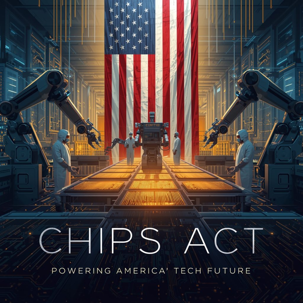
The CHIPS and Science Act of 2022 changed America’s industrial landscape overnight. What began as a bipartisan effort to restore supply-chain resilience and national security has become the backbone of a new era of advanced manufacturing — a policy that’s redrawing maps, reallocating billions, and redefining the nation’s technological independence. CHIPS at a Glance — What the Law Does and Why It Matters The CHIPS and Science Act authorized $52.7 billion in federal funding to rebuild the U.S. semiconductor ecosystem — spanning fabrication, R&D, and workforce training. Its centerpiece programs include: “CHIPS is not just about chips — it’s about reclaiming technological leadership.”— U.S. Department of Commerce, 2024 National Economic Impact — Jobs, Investment, and Industry Response The policy has ignited over $450 billion in announced private investments nationwide, according to industry trackers. Projects from Micron, Intel, GlobalFoundries, and TSMC have set off a construction and hiring boom. Analysts estimate 15,000 – 21,000 new semiconductor jobs and tens of thousands of indirect roles as suppliers and services expand. Beyond numbers, the CHIPS Act represents a re-anchoring of high-value manufacturing on U.S. soil — from wafers and materials to packaging and test. The ripple effects touch logistics, real estate, and education sectors, solidifying semiconductors as a national economic pillar. Global Context — Friendshoring and Tech Sovereignty The CHIPS Act is America’s answer to decades of strategic industrial policy in Asia and Europe. It signals a move toward friendshoring — aligning supply chains among allies while reducing overreliance on single regions. Similar programs are now active in the EU, Japan, and South Korea, signaling a global realignment of semiconductor geopolitics. Federal and State Programs Driving Growth The U.S. Department of Commerce’s CHIPS Incentives Program has awarded billions to projects including Micron ($6.16 B) and GlobalWafers ($406 M), supporting memory and wafer manufacturing. Simultaneously, state-level matching incentives — such as Texas’ Semiconductor Innovation Fund — amplify these federal grants to attract corporate investments. These layered policies reduce financial risk for multi-billion-dollar fabs while accelerating time-to-market — essential for staying competitive with Asia’s semiconductor giants. Austin’s Local Story — Turning Policy into Prosperity Austin stands as a clear beneficiary of the CHIPS Act’s momentum. Samsung’s Taylor Mega-Fab — a $17 billion investment — anchors Central Texas as a global semiconductor hub. The project is expected to generate thousands of construction and high-skill manufacturing jobs.Supplier Expansion — The CHIPS grant to GlobalWafers and Texas’ incentives for material suppliers have strengthened the regional ecosystem, cutting logistics costs and improving local capacity.Workforce Development — Partnerships between Austin Community College, University of Texas, and corporate sponsors are producing the next generation of fab technicians, engineers, and data specialists. “Austin’s semiconductor ecosystem isn’t just expanding — it’s accelerating innovation, education, and economic resilience.”— Austin Chamber of Commerce, 2025 Report Challenges and the Road Ahead Critics highlight the CHIPS Act’s high cost-per-job and the need for sustained workforce and supplier incentives. But its defenders call it strategic infrastructure — an investment in security, innovation, and sovereignty. To ensure long-term impact, policy analysts suggest three priorities: Conclusion The CHIPS Act has reshaped U.S. industrial policy and placed Austin at the heart of America’s semiconductor revival. Billions in public and private investment are now converging into tangible growth, skilled jobs, and technological momentum. Yet the real success will depend on sustaining that momentum — ensuring every dollar builds not just fabs, but a future-ready ecosystem.

State of the AR/VR Market — Size, Scope & Recent Advancements
Immersive Reality Reaches Industrial Maturity Once considered a playground for gamers and early adopters, Augmented Reality (AR) and Virtual Reality (VR) are now entering a new, transformative phase. As 2025 draws to a close, immersive technology has evolved from flashy demos to essential enterprise tools shaping how industries design, manufacture, train, and maintain complex systems. From Apple’s polished Vision Pro to Microsoft’s enterprise-grade HoloLens 2 and Meta’s mainstream Quest 3, the race for spatial computing dominance is fueling an ecosystem that bridges the physical and digital worlds.But beyond the consumer hype, the real story lies in the industrial adoption curve — where AR/VR is converging with AI, digital twins, IoT, and 5G to redefine productivity and collaboration. A Multi-Billion-Dollar Market Scaling at Breakneck Speed The global AR/VR market is expanding at a pace few other technologies can match.According to Global Growth Insights (2025), the sector is valued at roughly $92 billion in 2024 and is projected to reach $1.75 trillion by 2033, representing a stunning 38.7% CAGR.Even conservative estimates, such as Grand View Research, forecast steady double-digit growth well into the next decade. In hardware alone, Globe Newswire (2025) projects the AR/VR headset market to grow from $16.9 billion in 2025 to $261.9 billion by 2034, fueled by falling component costs, 5G connectivity, and AI-enabled spatial computing. In the manufacturing domain, the numbers are equally compelling: These figures highlight a tectonic shift — from entertainment to enterprise value creation. The Power Players Shaping the Next Reality The competitive landscape of immersive technology remains dynamic but is consolidating around a few influential players: Company Market Focus 2025 Market Share* Meta Platforms Consumer VR (Quest series), Metaverse ecosystem ~50% Apple Inc. Premium mixed reality (Vision Pro), spatial computing 10–15% Microsoft Corp. Enterprise AR (HoloLens 2), industrial deployment 8–10% XREAL / Nreal Lightweight AR glasses 10–12% Sony & HTC Gaming and enterprise VR 5–8% combined (Sources: TreeView Studio, 2025; Accio Analytics, 2024) While Meta continues to dominate on unit shipments, Apple’s Vision Pro has catalyzed premium demand and mainstream awareness. Microsoft maintains a stronghold in enterprise AR, where manufacturers, defense contractors, and aerospace firms use HoloLens for assembly guidance and remote collaboration. Emerging players such as XREAL, Magic Leap, and Vuzix are focusing on lightweight, see-through optics suitable for industrial and field applications — signaling the transition from “headsets” to everyday wearable interfaces. What’s Driving the Acceleration The new wave of AR/VR growth is being powered by a confluence of technological leaps and ecosystem readiness: Together, these trends are redefining the concept of “workspace.” The next decade will witness the emergence of immersive workplaces, where operators visualize data and collaborate seamlessly in 3D space. From Gaming to Grit: AR/VR’s Industrial Reinvention In manufacturing, immersive technologies are quietly becoming indispensable.Plant engineers, technicians, and quality teams are leveraging AR overlays to visualize maintenance steps, inspect deviations, and connect with remote experts in real time. Training & Skill Development A new generation of workforce training modules built in VR enables workers to experience hazardous or complex procedures without risk — cutting onboarding times by up to 40%. Maintenance & Remote Support Through AR glasses, technicians can follow guided repair workflows overlaid on real equipment, or connect with off-site specialists who annotate directly into their field of view. Downtime reductions of 20–30% are now common in pilot programs. Digital Twin Integration The integration of AR/VR with digital twin platforms lets operators “walk through” their factory’s virtual counterpart. Live process data from IoT sensors can be visualized spatially, enabling proactive maintenance, process optimization, and energy savings. Design & Simulation Before a single piece of equipment is installed, VR simulations allow engineers to review plant layouts, test ergonomics, and validate safety compliance. This approach has already reduced design rework by up to 25% in several advanced fabs. These capabilities are rapidly defining the Smart Manufacturing Metaverse — a convergence of AR/VR, AI, IoT, and automation that forms the foundation of Industry 5.0. Regional Momentum: Where Adoption Is Strongest As manufacturing hubs digitize globally, regional AR/VR strategies increasingly mirror national Industry 4.0 roadmaps. The Road Ahead: From Novelty to Necessity The next five years will witness the transition of AR/VR from niche pilot projects to standard operational infrastructure.Hardware will continue to miniaturize, software platforms will standardize, and AI will make immersive environments more intuitive and predictive. In this transformation, manufacturing stands out as the proving ground.AR/VR will not only train workers and reduce downtime but also enable new business models—remote commissioning, global design collaboration, and data-driven process optimization. For companies on the cusp of Industry 5.0, adopting immersive technologies is no longer experimental—it’s existential. Key Takeaways In Closing As digital transformation reshapes every industrial sector, immersive reality is emerging as the next universal interface—one that connects engineers, operators, and data in a single, spatially intelligent environment. The winners of this new era won’t be those who simply build more powerful headsets, but those who embed immersive intelligence into everyday manufacturing workflows—turning data into experience, and experience into advantage. (End of Feature – © 2025 Austin ChipFrontier Magazine – “Connecting Innovators and Building Futures.”)

Inside the AI Infrastructure Explosion: Data Centers, Chips, and the Race for Compute Power
The global data center industry is in the middle of a rare, high-velocity expansion. What started as steady growth to support cloud services and streaming has become an industrial-scale build-out driven by the compute needs of modern artificial intelligence (AI). The result: an enormous appetite for power, racks, networking and — critically — semiconductors, especially high-performance accelerators. Below I explain the demand drivers, how AI and data centers are tightly coupled, and the downstream impacts on semiconductor technology and supply chains. This is written in a LinkedIn-ready format so you can share it with colleagues and stakeholders. The boom: what’s fueling it Three forces combine to explain why data centers are growing faster than at almost any time in recent memory: The practical implications are visible: siting decisions now consider grid capacity and latency for model training clusters, not just land and fiber; liquid cooling and new rack designs are being adopted; and some regions (e.g., parts of Texas) report massive interconnection requests tied to these projects. How AI and data centers are connected (why one can’t grow without the other) AI workloads are compute-bound rather than storage- or I/O-bound. Training large models scales roughly with compute × time, and leading models are trained on thousands of GPUs in parallel. That drives three critical changes in data center design: Put simply: AI dictates what data centers are (high-density compute factories), and data centers provide the physical infrastructure AI needs to scale. The semiconductor ripple effects The demand shock at data centers translates directly into winners, losers and accelerated technical trends across the semiconductor landscape. 1. Surging demand for accelerators (GPUs, TPUs, IPUs, and ASICs) GPUs (NVIDIA et al.) and other AI accelerators are the dominant consumables for AI compute. These devices have become the single largest driver of data-center semiconductor revenue and capacity planning: companies report record data-center segment revenue tied to AI products. That increases foundry orders for advanced logic nodes and places sustained near-term pricing power in the hands of a few firms. 2. Foundry capacity and node priorities shift Advanced nodes (3nm, 2nm and beyond) are prioritized for high-performance accelerators and high-margin logic. That means wafer fabs, packaging lines and advanced test capacity are being allocated in favor of AI chipmakers — pressuring commodity segments and legacy nodes in different ways. Industry forecasts and analyst reports show meaningful revenue reallocation and a steeper top-end concentration of economic profit among the leading semiconductor firms. 3. Advanced packaging and chiplets accelerate As power, heat and yield limits make monolithic scaling harder, customers are moving to advanced packaging (2.5D/3D stacking, interposers, chiplets) to increase performance and modularity. Packaging vendors and OSATs (outsourced semiconductor assembly/test) are expanding capacity to serve the data-center accelerator market. This trend reduces dependence on single huge dies and favors ecosystems that combine compute chiplets, HBM memory stacks and high-bandwidth interconnects. 4. Supply chain stress and geopolitics Concentrated demand for a narrow set of chips amplifies supply-chain bottlenecks: wafer supply, advanced EUV masks, HBM memory, and substrate materials. Governments and companies are responding with capex (new fabs, sovereign supply initiatives) and policy interventions to secure capacity. Expect continued elevated investment in domestic fabs and diversified supplier footprints. 5. Power, cooling and thermal materials market growth Chip performance rises require new cooling solutions (direct liquid, immersion cooling) and thermal interface materials — which in turn create demand for materials science innovation and new suppliers to serve data-center customers. This is a non-trivial secondary market that benefits companies outside the standard silicon supply chain. Strategic takeaways for industry leaders Conclusion The data-center boom is not a simple real-estate story — it’s a compute story. AI is reshaping what data centers need and where semiconductor industry dollars flow: toward accelerators, advanced nodes, packaging innovations, and the energy/thermal ecosystems that make sustained high-density compute possible. For executives, investors and technologists, the message is clear: AI-driven demand is remaking both the brick-and-mortar infrastructure of computing and the silicon supply chains that power it. Those who align design, manufacturing and facilities strategies to this new reality will shape the economics of the next decade.
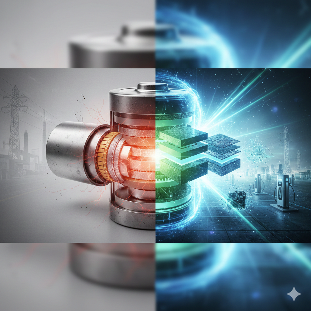
After Lithium: Why Advanced Batteries Will Define the Next Decade of Energy Storage
The lithium-ion battery has been the cornerstone of the mobile revolution—powering everything from smartphones to EVs. But the era of lithium dominance is reaching its limits. Supply constraints, safety concerns, and performance ceilings have opened the door for new chemistries and architectures to redefine what’s possible in energy storage. Across labs and industries, the race is on. Solid-state, sodium-ion, lithium-sulfur, and metal-air batteries are no longer distant dreams. They are materializing into commercial realities—bringing with them the potential to reshape the economics of energy, transform national security strategies, and enable the next wave of electrification at the grid scale. The Limits of Lithium-Ion While lithium-ion batteries (LIBs) have seen remarkable improvements in energy density and cost reductions—falling from $1,200 per kWh to under $150 per kWh in the last decade—there are fundamental limits that cannot be engineered away. Current data suggests that LIBs are approaching their theoretical energy density ceiling (~300 Wh/kg), and incremental gains are becoming harder and more expensive to achieve. Moreover, lithium’s geopolitical complexity is intensifying. According to recent industry benchmarks, over 60% of lithium refining capacity is concentrated in China, presenting vulnerabilities for markets dependent on secure battery supply chains. Cobalt and nickel, often used in LIB cathodes, pose similar risks—both in ethical sourcing and pricing volatility. Emerging Chemistries: What’s Next? Here’s a breakdown of the most promising post-lithium contenders: Each of these technologies represents a tradeoff—between energy density, cost, cycle life, and manufacturability. But the overarching trend is clear: we are moving toward a more diversified battery landscape, optimized for use-case rather than a one-size-fits-all approach. Architectural Shifts and Manufacturing Scalability It’s not just about new chemistries. The architecture of battery cells—pouch vs. prismatic, anode-free designs, 3D current collectors—is evolving rapidly. Startups like Sila Nanotechnologies and Group14 are deploying silicon-dominant anodes to boost capacity without overhauling OEM lines. Simultaneously, dry-electrode manufacturing (pioneered by companies like Tesla and Maxwell Technologies) promises to cut energy use during production by up to 90%. Scalability remains the bottleneck. According to recent industry benchmarks, less than 5% of global battery production capacity is currently geared for anything other than lithium-ion. That means billions in retooling—and a multi-year ramp-up—before alternatives can compete at scale. However, policy tailwinds like the U.S. Inflation Reduction Act and the EU Battery Regulation are accelerating this transition. Key Market Implications The Economic Stakes The battery industry is expected to exceed $400 billion by 2030, according to BloombergNEF. But beyond size, it’s the strategic leverage that matters. Advanced batteries will dictate who controls the clean energy transition—who builds the next Tesla, who dominates grid storage, who maintains digital sovereignty as AI and edge computing become increasingly mobile. For energy companies, automakers, and even cloud providers, batteries are no longer a component. They are a strategic fulcrum. Conclusion We are standing at the edge of a new battery paradigm—where the question is no longer “How do we improve lithium-ion?” but “What comes after it?” The answers will determine not only who leads in energy and mobility but who wins the broader industrial game over the next decade. What’s your take—will advanced batteries disrupt the energy status quo faster than we expect, or will lithium remain the incumbent for longer than most forecasts suggest?
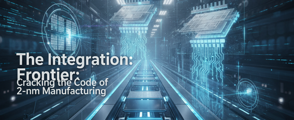
Inside the 2-nm Revolution: How Process Integration Defines the Next Breakthrough
Feature Story | Advanced Nodes & Integration Challenges “At 2 nanometers, the transistor is no longer the star — the orchestra of integration is.” The semiconductor industry’s sprint from 7 nm → 5 nm → 3 nm looked like a steady continuation of Moore’s law. But the 2-nanometer class is a different beast altogether — not just a shrink, but a tectonic re-engineering of everything from device architecture and power delivery to materials and yield learning. In this race, process integration — the invisible glue binding thousands of unit steps — determines who wins commercial success and who drowns in cost and complexity. Why 2 nm Is Not a Routine Step At 2 nm, the industry is shifting from FinFETs to Gate-All-Around FETs (GAAFETs) — Samsung’s MBCFET, Intel’s RibbonFET, and TSMC’s nanosheet GAA.GAA devices promise better electrostatics and performance-per-watt efficiency, but introduce a daunting level of process choreography: atomic-level control over sheet thickness, sacrificial layer removal, stress engineering, and backside power delivery. “It’s not a new transistor; it’s a new philosophy of manufacturing.” Each of these steps must align flawlessly — across thousands of masks, depositions, etches, and CMP stages — to yield functional wafers. Integration Challenges: Where Physics Meets Reality 1. Device complexity & razor-thin process windows Stacked nanosheets demand sub-ångström control. Even minute deviations in thickness or strain shift threshold voltages, destroying yield. IMEC researchers have repeatedly warned that nanosheet strain control and source/drain consistency are the Achilles’ heel of GAA integration. 2. Lithography: EUV alone isn’t enough At 2 nm, EUV still needs multi-patterning, extreme overlay precision, and defect-free masks. High-NA EUV promises better resolution, but introduces new metrology hurdles and escalating tool costs. “One speck of defect can wipe out an entire wafer.” 3. Backside power delivery & thermal limits TSMC’s PowerVia and Intel’s PowerVia approaches bring power rails to the wafer’s backside — reducing IR drop but introducing wafer thinning, warpage, and new yield loss mechanisms. 4. BEOL & contact resistance bottlenecks Shrinking dimensions make interconnect resistance the new limiter. Even perfect transistors can be bottlenecked by BEOL RC delays unless new barrier and single-grain metal stacks are perfected. 5. Defects, yield curves & supply pressure Every integration tweak spawns new defect modes. TSMC’s reported defect-density trends for N2 are promising, but each step forward demands unprecedented in-line metrology and root-cause analytics. 6. Packaging co-design At 2 nm, packaging becomes a first-order design parameter. Chiplets, TSVs, and interposers must thermally and mechanically align with ultra-thin dies. Supply Chain & Tool Dependencies Beyond physics, there’s a geopolitical and logistical battlefield.High-NA EUV tools from ASML are scarce and massive, advanced mask blanks are limited, and qualified integration engineers are in short supply. The capex per fab is ballooning — pushing smaller foundries out and forcing mega-foundries (TSMC, Intel, Samsung) to secure long-term partnerships across the entire supply stack. “Integration isn’t done in a cleanroom alone — it’s a global coordination act.” Timeline: The 2-nm Race So Far Year Milestone Key Player Jul 2021 Intel launches “Angstrom Era” roadmap with RibbonFET & PowerVia Intel Oct 2021 Announces 2 nm-class MBCFET (2GAP) roadmap Samsung Apr 2022 TSMC reveals N2 nanosheet GAA + backside power roadmap TSMC 2022–2023 IMEC publishes nanosheet and forksheet integration studies IMEC 2024–2025 Risk production and 2-nm tape-outs by key customers TSMC / MediaTek 2025 Defectivity data show steady improvement toward HVM TSMC / Samsung What “Success” Looks Like To make 2-nm commercially viable, foundries must: “In 2-nm, process integration is not a department — it’s the business model.” Bottom Line The promise is clear: 10–15% performance boost, 20–30% power reduction, and potentially 50 billion transistors per chip.But the cost of a misstep is even higher. The first foundry to balance performance, yield, and cost will define the next decade of computing. 2 nm is not just smaller — it’s smarter, harder, and far less forgiving. Further Reading Top of Form Bottom of Form