


For decades, the semiconductor industry followed a clear path: shrink the node, boost performance, reduce power. But that roadmap, defined by Moore’s Law, is hitting a wall—not just physically, but economically.
At 3nm and below, the cost per transistor is no longer dropping significantly. Design complexity has skyrocketed. Yields are pressure points. Meanwhile, foundries and fabless players are rewriting the playbook—not around smaller nodes, but smarter integration.
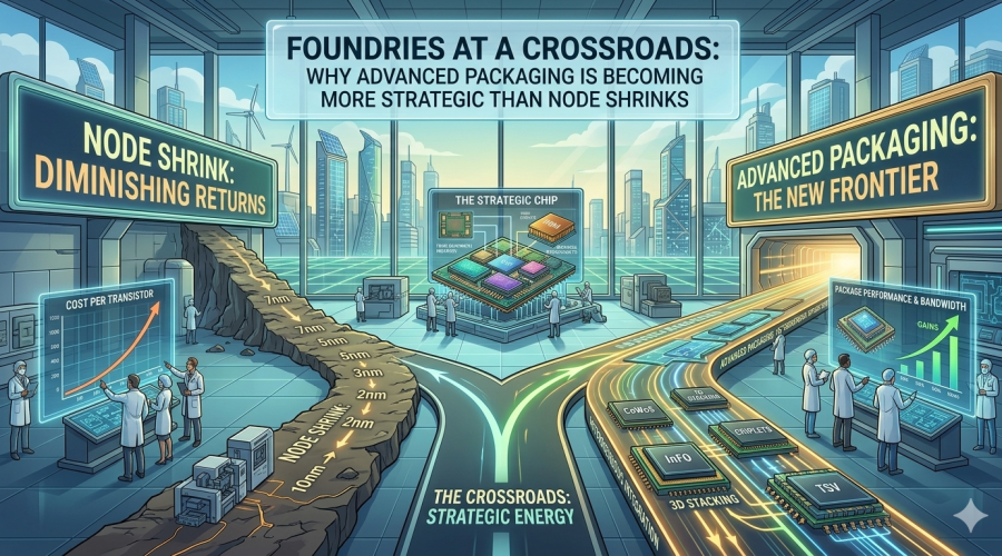
Enter advanced packaging.
Once a back-end consideration, packaging is now a front-line differentiator. Chiplets, 2.5D, 3D stacking, and hybrid bonding are reshaping how performance and power efficiency are achieved.
Why This Matters Now
Advanced packaging is enabling performance gains that rival—and sometimes exceed—those from full-node shrinks, without the escalating cost curve.
According to recent industry benchmarks, chiplet-based designs can reduce time-to-market by 30% and lower development costs by up to 50% compared to traditional SoC approaches at leading-edge nodes.
Apple’s M-series chips, AMD’s EPYC line, and Intel’s Foveros architecture are all leveraging these techniques to combine IP blocks fabricated on different process nodes. The results? Higher bandwidth, lower latency, better thermal profiles—without waiting on the next process technology to mature.
Key Insights
- Node economics are shifting: Below 7nm, each shrink delivers diminishing returns in cost-per-transistor and power efficiency.
- Chiplets unlock modular scaling: Reusing validated IP across multiple products reduces verification overhead and speeds deployment.
- Vertical integration is back: Leading foundries are investing in packaging capabilities to offer end-to-end design and manufacturing services.
- Thermal and interconnect challenges are design drivers: Packaging now plays a pivotal role in managing power density and data flow.
- Supply chain implications: Outsourced packaging and testing (OSAT) vendors are racing to keep up, but leading-edge capabilities are consolidating among top-tier foundries.
Market Implications
Current data suggests that by 2027, more than 50% of advanced node chips will use some form of heterogeneous integration. The shift is real—and irreversible.
Foundries that once competed on nanometers now compete on packaging roadmaps. TSMC’s CoWoS and InFO, Intel Foundry Services’ EMIB and Foveros, and Samsung’s X-Cube are all signaling a broader pivot: packaging is no longer a commodity—it’s the next frontier of innovation.
This evolution will reshape semiconductor competition, capital allocation, and design strategies. It also creates new opportunities for EDA players, substrate suppliers, and thermal engineers to claim a more strategic seat at the table.
We’re seeing the dawn of a new paradigm where performance per watt per mm2 is optimized not just through silicon scaling—but through architectural ingenuity and packaging intelligence.
Final Thought
As Moore’s Law slows, More-than-Moore accelerates. The question isn’t just who can build the smallest transistors—but who can assemble the smartest systems.
Is your organization investing in packaging innovation as aggressively as it once did in node shrinks?
#Semiconductors #AdvancedPackaging #Chiplets #MooresLaw #FoundryStrategy #HeterogeneousIntegration #AIHardware