

The semiconductor industry is undergoing a tectonic transformation. As Moore’s Law approaches its physical and economic limits, chiplet-based heterogeneous integration is emerging not as a stopgap, but as a foundational strategy for next-generation semiconductor design.
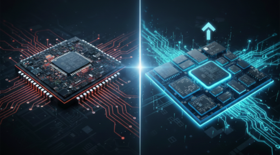
Instead of building massive monolithic dies on leading-edge process nodes like 3nm or 5nm—an increasingly costly endeavor—designers are now disaggregating system-on-chips (SoCs) into modular chiplets. These chiplets, each optimized for specific functions and fabricated on the most suitable process nodes, are then integrated into a single package using advanced interconnect technologies like silicon interposers or embedded bridges.
Why this matters now
Current data suggests that designing a monolithic SoC on a 3nm node can cost upwards of $500 million in NRE (non-recurring engineering) expenses. In contrast, chiplet-based architectures enable reuse of IP blocks, allow mixing of mature and advanced nodes, and drastically reduce design cycles and manufacturing risk. This is not just an engineering win—it’s a business imperative.
Consider the AMD EPYC processors or Intel’s Foveros 3D stacking: both employ chiplet strategies to achieve stunning performance-per-watt metrics, while keeping yields and costs in check. AMD, for instance, uses 7nm chiplets for cores and a 14nm I/O die, optimizing for performance and cost simultaneously.
Technical Edge
Heterogeneous integration is not just about cost—it’s also about performance scaling beyond silicon shrinkage. By combining high-bandwidth memory (HBM), AI accelerators, and general-purpose cores in one tightly integrated package, chiplet architectures reduce latency and power consumption across data paths. For AI and HPC workloads, where interconnect latency and memory bandwidth often become bottlenecks, this design philosophy is a game-changer.
According to recent industry benchmarks, chiplet-based designs can improve interconnect speeds by up to 2x while reducing power per bit by over 40% compared to conventional board-level integration.
Key Implications
- Cost Optimization: Reusing proven IP chiplets across multiple product lines reduces development costs and speeds time-to-market.
- Node Agnosticism: Enables mixing mature nodes (e.g., 28nm, 14nm) with cutting-edge nodes (e.g., 5nm, 3nm), creating optimal performance-cost trade-offs.
- Design Agility: Modular architectures simplify variant creation for different markets—consumer, automotive, datacenter, etc.
- Supply Chain Resilience: Decoupling functional blocks means sourcing from multiple fabs, improving availability and mitigating risk.
- AI Acceleration: Chiplet designs are ideal for embedding specialized AI cores with low-latency paths to memory and compute components.
For semiconductor startups and hyperscalers alike, this changes the playbook. Instead of investing billions into building end-to-end SoCs, companies can focus on domain-specific chiplets and participate in a collaborative ecosystem. This democratizes hardware innovation and enables faster deployment cycles for AI, 5G, and edge computing solutions.
A New Silicon Economy
As chiplet standardization efforts like UCIe (Universal Chiplet Interconnect Express) gain traction, we’re looking at the rise of a modular silicon economy—where chiplets become the IP blocks of the future, traded and integrated much like software APIs today.
This is not just the next phase of semiconductor evolution; it’s a re-imagining of how chips are designed, built, and delivered.
What would your product roadmap look like if silicon became as modular—and as agile—as software?
#Chiplets #Semiconductors #HeterogeneousIntegration #AIHardware #AdvancedPackaging #MooresLaw