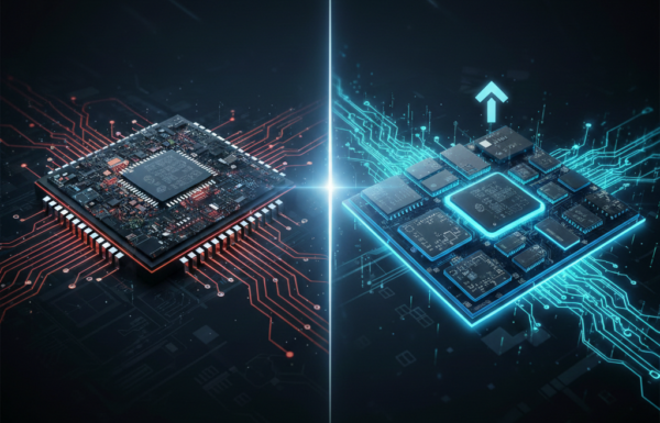
The semiconductor industry is undergoing a tectonic transformation. As Moore’s Law approaches its physical and economic limits, chiplet-based heterogeneous integration is emerging not as a stopgap, but as a foundational strategy for next-generation semiconductor design. Instead of building massive monolithic dies on leading-edge process nodes like 3nm or 5nm—an increasingly costly endeavor—designers are now disaggregating system-on-chips (SoCs) into modular chiplets. These chiplets, each optimized for specific functions and fabricated on the most suitable process nodes, are then integrated into a single package using advanced interconnect technologies like silicon interposers or embedded bridges. Why this matters now Current data suggests that designing a monolithic SoC on a 3nm node can cost upwards of $500 million in NRE (non-recurring engineering) expenses. In contrast, chiplet-based architectures enable reuse of IP blocks, allow mixing of mature and advanced nodes, and drastically reduce design cycles and manufacturing risk. This is not just an engineering win—it’s a business imperative. Consider the AMD EPYC processors or Intel’s Foveros 3D stacking: both employ chiplet strategies to achieve stunning performance-per-watt metrics, while keeping yields and costs in check. AMD, for instance, uses 7nm chiplets for cores and a 14nm I/O die, optimizing for performance and cost simultaneously. Technical Edge Heterogeneous integration is not just about cost—it’s also about performance scaling beyond silicon shrinkage. By combining high-bandwidth memory (HBM), AI accelerators, and general-purpose cores in one tightly integrated package, chiplet architectures reduce latency and power consumption across data paths. For AI and HPC workloads, where interconnect latency and memory bandwidth often become bottlenecks, this design philosophy is a game-changer. According to recent industry benchmarks, chiplet-based designs can improve interconnect speeds by up to 2x while reducing power per bit by over 40% compared to conventional board-level integration. Key Implications Cost Optimization: Reusing proven IP chiplets across multiple product lines reduces development costs and speeds time-to-market. Node Agnosticism: Enables mixing mature nodes (e.g., 28nm, 14nm) with cutting-edge nodes (e.g., 5nm, 3nm), creating optimal performance-cost trade-offs. Design Agility: Modular architectures simplify variant creation for different markets—consumer, automotive, datacenter, etc. Supply Chain Resilience: Decoupling functional blocks means sourcing from multiple fabs, improving availability and mitigating risk. AI Acceleration: Chiplet designs are ideal for embedding specialized AI cores with low-latency paths to memory and compute components. For semiconductor startups and hyperscalers alike, this changes the playbook. Instead of investing billions into building end-to-end SoCs, companies can focus on domain-specific chiplets and participate in a collaborative ecosystem. This democratizes hardware innovation and enables faster deployment cycles for AI, 5G, and edge computing solutions. A New Silicon Economy As chiplet standardization efforts like UCIe (Universal Chiplet Interconnect Express) gain traction, we’re looking at the rise of a modular silicon economy—where chiplets become the IP blocks of the future, traded and integrated much like software APIs today. This is not just the next phase of semiconductor evolution; it’s a re-imagining of how chips are designed, built, and delivered. What would your product roadmap look like if silicon became as modular—and as agile—as software? #Chiplets #Semiconductors #HeterogeneousIntegration #AIHardware #AdvancedPackaging #MooresLaw
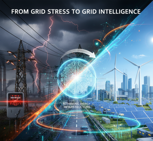
From Grid Stress to Grid Intelligence: How Renewables Are Forcing a Rethink of Energy Infrastructure
The energy transition is no longer a distant goal—it’s a present imperative. As the share of solar, wind, and other intermittent renewables on the grid grows, utilities and grid operators are navigating an increasingly complex, volatile, and decentralized energy landscape. What’s at stake? Not just reliability, but the future of energy economics itself. Traditional grids were built for unidirectional power flow: large centralized plants generating electricity, which flows to passive consumers. That model is breaking down. Now, millions of distributed energy resources (DERs)—from rooftop solar to EV chargers—are pushing power back into the grid. This bidirectional flow is making the grid behave more like a dynamic network than a linear system. According to recent industry benchmarks, in regions like California and parts of Europe, renewables already contribute more than 30% of total electricity generation annually. On some days, they exceed 100% of instantaneous demand. While this marks a win for sustainability, it introduces unprecedented stress on infrastructure designed decades ago. The Case for Grid Intelligence To orchestrate an increasingly complex supply-demand equation, utilities are embracing a new paradigm: grid intelligence. This is not simply about adding sensors or analytics layers—it’s about re-architecting the grid with AI, edge computing, and real-time control systems. Modern intelligent grids incorporate: Advanced Distribution Management Systems (ADMS): Integrating DERs in real-time with predictive analytics to forecast load and generation. Latency-optimized edge computing: Managing microgrid operations and resilience locally, with sub-100ms response times. AI-based forecasting algorithms: Leveraging weather, consumption, and historical data to anticipate load patterns and renewable availability. Solid-state transformers: Offering voltage control and bidirectional power flow for managing variable energy inputs. Grid-forming inverters: Enabling renewables to provide synthetic inertia and enhance grid stability. The Semiconductor Backbone Grid intelligence is not just a software problem—it’s a hardware challenge too. Semiconductors are playing a pivotal role in the energy transition. Power-efficient chips at 7nm and below are powering real-time analytics at the grid edge, while wide-bandgap materials like SiC and GaN are driving high-efficiency power conversion in inverters and EV chargers. Current data suggests that the market for power semiconductors in energy infrastructure will surpass $10B by 2026. This is catalyzing innovation across the supply chain—from chip architecture to thermal management systems and new packaging standards. Key Insights Legacy grid architecture is fundamentally incompatible with high-penetration renewables. Grid intelligence enables real-time responsiveness, resilience, and economic optimization of energy flows. AI and edge computing are critical for managing the volatility introduced by DERs. Semiconductor innovation is essential to enable low-latency, high-efficiency energy systems. Utilities that fail to invest in grid intelligence risk escalating O&M costs and systemic instability. So What? The industrial implications are profound. Grid modernization is not just a technical upgrade—it’s a competitive necessity. Utilities that adopt intelligent infrastructure will not only ensure grid reliability but also unlock new revenue streams through demand response, flexible pricing, and energy-as-a-service models. Conversely, those that fail to adapt risk stranded assets and regulatory penalties. Investors, OEMs, and policymakers should be watching closely. The next decade will determine whether today’s grid stress becomes tomorrow’s crisis—or catalyst. Are we ready to move from grid resilience as a reaction, to grid intelligence as a strategy? #GridIntelligence #RenewableEnergy #EnergyTransition #SmartGrid #PowerSemiconductors #CleanTech #InfrastructureInnovation
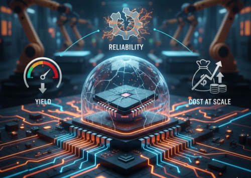
The Real Bottleneck in Advanced Semiconductors: Yield, Reliability, and Cost at Scale
The Real Bottleneck in Advanced Semiconductors: Yield, Reliability, and Cost at Scale As the semiconductor industry races toward sub-3nm nodes and heterogeneous integration, attention often gravitates toward breakthrough transistor architectures, extreme ultraviolet (EUV) lithography, or AI-specific chip designs. But those watching only the front-end innovations may be missing the real bottleneck: yield, reliability, and cost at scale. At 3nm and below, every part of the manufacturing chain—from mask complexity to process variability—introduces exponentially greater risk. And while the headlines celebrate smaller transistors and faster chips, the hard truth is this: producing those chips reliably and affordably, in volume, is the true challenge. Why Yield and Reliability Have Become the Battlefield In the 28nm era, process maturity meant yields regularly exceeded 90%. Fast forward to 5nm and below, and even industry leaders are grappling with yields in the 50–70% range for complex SoCs. At 3nm, with GAA (Gate-All-Around) structures and increased parasitic coupling, variability becomes a nanoscopic minefield. A minor process deviation can scrap entire wafers. Current data suggests that the cost per good die at 3nm is nearly 50% higher than at 5nm—not due to raw fab costs alone, but because of lower yields and increased post-processing requirements. And with advanced packaging (e.g., 2.5D, 3D HBM stacks), the failure rate compounds across the system level. The Reliability Conundrum As chips shrink, their susceptibility to electromigration, soft errors, and thermal hotspots rises. Reliability isn’t just a concern for automotive or aerospace anymore—it now affects AI data centers, where downtime directly translates to multimillion-dollar losses. According to recent industry benchmarks, AI accelerators running large transformer models (100B+ parameters) require sustained uptime to justify TCO. Even a 0.1% drop in reliability across tens of thousands of GPUs can result in delays and lost inference throughput—undermining SLAs for hyperscalers. The Cost Scaling Myth Moore’s Law promised cost-per-transistor reductions with each node shrink. That promise is cracking. While transistor densities are indeed increasing, the cost per die isn’t falling in step. In fact, the average wafer cost at 3nm is estimated to be 30–40% higher than at 5nm—before accounting for yield losses. This shifts the economic calculus: is performance-per-watt still worth the massive capex and yield risk? For some workloads—like high-throughput AI training—the answer may still be yes. But for many edge and consumer applications, older nodes with improved packaging might deliver better ROI. Key Insights Yield degradation at advanced nodes (3nm and below) is becoming the dominant cost factor—more than raw wafer pricing or EUV capex. Reliability risks now affect not just safety-critical systems, but AI data centers operating at hyperscale intensity. Advanced packaging introduces new failure points, compounding cost and complexity at the system level. Economic scaling is diverging from transistor scaling—raising tough questions for system architects and CFOs alike. Legacy nodes with better packaging may outperform bleeding-edge nodes in cost-sensitive or thermally constrained applications. Market Implications Companies betting on AI accelerators, HPC chips, or next-gen mobile SoCs must now factor not just PPA (power, performance, area)—but YRC: Yield, Reliability, and Cost. For foundries, this creates a bifurcation: high-value customers will absorb the costs of advanced nodes, but a growing segment of the market may revert to N+1 or N+2 nodes with innovative chiplet designs. TSMC’s 6nm and 7nm lines remain in high demand for this reason. For system designers, the focus shifts from just “what node?” to “what architecture, packaging, and yield model delivers the best ROI?” Engineering excellence must now extend into manufacturing science and supply chain economics. Looking Ahead The semiconductor narrative is evolving. It’s no longer just about nanometers—it’s about predictability, durability, and economic viability at scale. As we design chips to power trillion-parameter AI models and autonomous systems, we must also design for manufacturability and reliability at global scale. What if the real innovation in semiconductors isn’t at 2nm—but in how we better scale 7nm with smarter yield strategies and reliability engineering?